Process window
Table of Contents
- What is process window?
- How to improve the process window?
- What can designers learn from process-window optimization?
The semiconductor industry is absolutely relentless in technological advancements, constantly adopting new technologies, processes and materials just to scale further. Often misunderstood is that this scaling is not just in nanometers, but also economically. A company can scale in nanometers like no other, but still lose the race to a competitor if they don’t achieve the right economics.
For the economics to work out, we often talk about Yield. Yield is the percentage of chips that meet the desired specifications, thus a higher percentage means more working chips. Looking at recent numbers for advanced packaging between three fierce competitors, Intel, Samsung Electronics and TSMC, their processes yield at 90%, 50% and 98% respectively [source].
Increasing Yield is everything in a successful semiconductor node. So let’s look at a critical concept in increasing yield, process window.
What is process window?
Process window is very simply the range of values for a given parameters that yields an acceptable result of the process.
To give an example, in a photo-lithography system the printed features have a focus dependence, which changes the printed dimensions when moving through focus. The focus has an acceptable range that still results in features printed which give an acceptable result and produce a functioning chip. The operating focus offset can be within let’s say [-20um, +20um] from focus, which will give a different feature size printed, but acceptable enough.
This principle applies not just to focus of a lithography system, but of nearly every parameter in every process step, and finding these process windows and learning how to increase the process window are crucial.
How to improve the process window?
One way to increase the process window is to reduce the sensitivity of a given parameter’s impact on a given feature. This can be by optimizing where we operate, for example if there is a parabolic dependency as such:
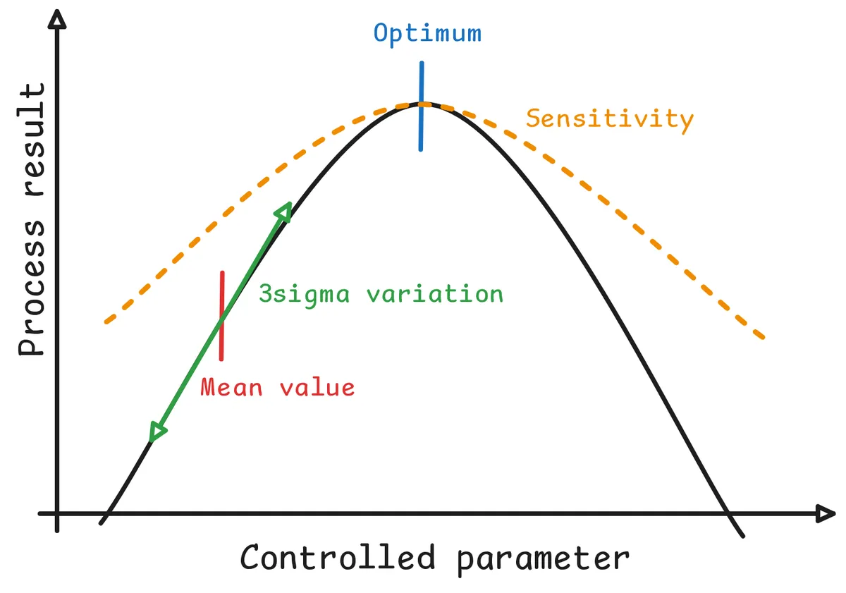
Operating in any part away from the peak of the parabola, makes you more sensitive to changes in the physical parameters governing the lithography process, and thus giving you a less consistent result. In the end we are dealing with physical systems, pushed to the absolute limit of human engineering over the past 60 years, and thus even the smallest disturbances can create a variation on the end result. Take Typhoons, even the slight difference in air-pressure from a typhoon a modern semiconductor plant a week in advance, is enough to disturb the process result. Modern lithography systems are almost indirect sensors of the tiniest meteorological or natural phenomena. So it’s absolutely crucial to try and operate at a point in your process window where you are least sensitive to disturbances, meaning the flat part of the curve.
This is also the operating principle behind ULE and Zerodur. Both being types of glass, with near zero thermal expansion coefficients in a specific temperature range. Stay within that temperature range, and the material barely deforms (shrinking or growing) with changing temperatures. It’s no wonder that these materials are also heavily used in Lithography systems which require extreme material control to achieve nanometer level of precision. If you can keep these materials on average close to the optimal temperature where the thermal expansion curve is flat, then it will be very insensitive to thermal changes, helping improve your process window.
Another way to optimize your process window is to flatten your curve, decreasing your sensitivity. Of course this is the engineering that went into developing Zerodur and ULE. However, I favour another example for this. Not from the world of lithography, but from etching.
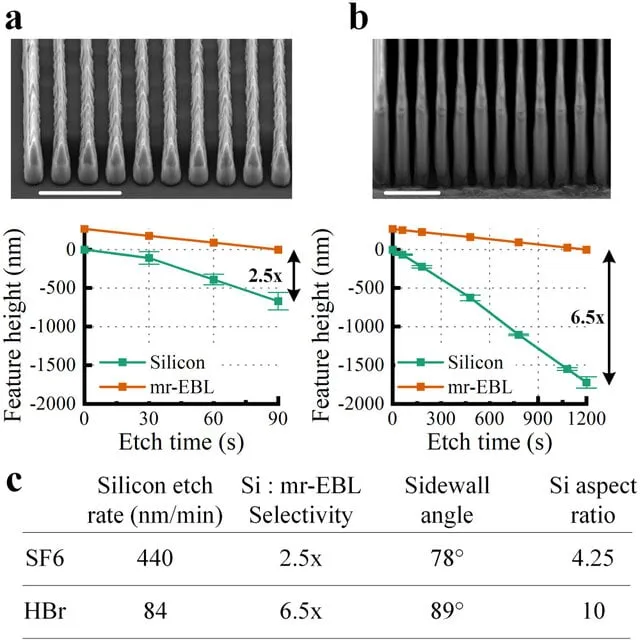
Etching is the selective removal of material based on some defined pattern. The pattern is created by the lithography process, but etching is how the physical structures actually get created. Etching nowadays is mostly done through plasma-enhanced chemical etching. Meaning a certain gas composition is ignited into a plasma, and accelerated towards the silicon wafer. These accelerated ions bombard the wafer and provide the thermal energy required for chemical reactions to take place at the wafer surface. Because these are chemical processes, governed by activation energies (a certain amount of energy needs to be put into the pre-reactions to break the necessary chemical bonds), only a select few reactions can take place. This will then selectively remove material from the wafer surface. This is the principle behind Reactive-Ion Etching (RIE).
The selectivity of this process is a very important parameter, it determines how much material of the silicon wafer is removed compared to the etching mask, the protective layer defined in the lithography process. The higher the selectivity, the less sensitive you are to process variations.
Changing the selectivity of an etching process often comes down to changing the chemistry. Switching to different gas composition in the etching reaction chamber. What’s important to note about this is that to improve the process sensitivity, quite a fundamental design change is made, changing which chemical reactants are responsible for the etching. This is often the case with reducing the sensitivity, it requires material or design changes fundamental to the process, and cannot be achieved with tighter control or parameter changes.
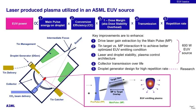
The final knob we have for increasing our process window is to have tighter control over the process. To reduce the variations of the parameter that affects our end result, often measured in the 3-sigma value of the controlled parameter. This is often simpler than it looks, and can take a non-trivial amount of effort and time to improve. Take the example of the 600W EUV Source. For this new generation source, one of the key improvements is enhanced stability of the EUV generation process, partially driven by increased stability of the 1um laser architecture compared to the previous 10um laser architecture.
The reason for this improvement is conceptually simple, steering and controlling a 30kW laser system is much more challenging than the ~300W 1um laser system used on the latest generation EUV systems. This still requires a complete re-imagining of the EUV Source to achieve however, and took years for ASML to develop and roll-out to their customers.
What can designers learn from process-window optimization?
Process window is something that is always in the back of the mind of the chipmakers’ engineers. It’s arguably one of the reasons TSMC is a cut above their competitors, just because of how hard they push on this, all throughout their supply chain.
So there are a few questions that every designer should ask themselves as frequently as possible, namely:
- What are my sensitivities, and where do they originate from?
- How do I reduce noise in my system?
- How do I ensure I’m operating as close to the optimum at all time?